|
both uniform compositions
and layered structures for NPN transistors. They were making point contact
diodes and transistors, NPN grown junction transistors, and later PNP
transistors (including my power transistors), and alloy junction high
voltage diodes. I was involved with
most of these operations, but I didn’t have any management responsibility.
I also remember details of
the basic equipment used for reduction of germanium dioxide to germanium,
zone leveling, crystal growth, sawing, grinding, etching, dicing,
encapsulation, etc, since the place wasn’t very big and I had some hands-on
experience with all this equipment.
This was basic to the diode and NPN transistor programs that were
running in 1953 when I was first involved.
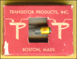
As I recall it, the main products at the time were point contact
transistors, UHF diodes, and grown junction NPN transistors, with a start
made on PNP alloy junction transistors.
Much of the work was guided
by several thick manuals published by Bell Labs. I can’t remember much detail of what was in them.
As with most TP products,
the point contact transistors were made on a fairly “manual” production
line and then were adjusted and had the point contacts “formed” (by
discharging a capacitor) at the end.
After this, they were tested and sorted into
|