|
EARLY TRANSISTOR
AND DIODE HISTORY AT BELL LABS Art Uhlir Jr. |
||
|
Oral History – Art Uhlir Jr. (Continued) |
|
|
|
Your early work at BTL with varactor diodes and parametric
amplifiers has been tremendously influential in the electronics industry over
the past 50 years. Recently, there has been substantial interest in another
of your early discoveries known as porous silicon. What are your comments on
that? My wife Inge and I were invited to give the opening address March
15 at the 2004 PSST (Porous Semiconductor Science and Technology) conference)
in Cullera, Spain. Fifty years earlier we discovered a curious substance
produced by electrolytic etching in HF solution of the first silicon single
crystal made available to us. This discovery was sort of a parting shot on
leaving electrochemical machining of germanium and common metals. It was an axiom of early transistor technology that mechanical
damage produced by sawing and lapping should be removed by chemical etching. The etching of crucible-grown germanium
floating-zone crystals had been correlated with low point-contact transistor
yields from the corresponding region.
The etch pits were cheerfully heralded as evidence of the dislocations
predicted by W. T. Read. Electrolytic
etching in KOH solution gave more lurid pits. Go
To Uhlir Oral History, Page 13 |
|
|
|
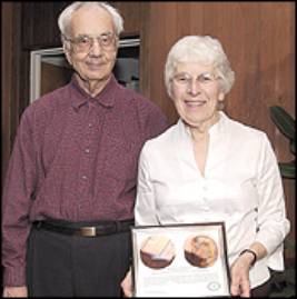
This is a recent photo of Art Uhlir Jr. and his
wife, Inge, holding the award presented to them at the 2004 PSST Conference
in Valencia Spain, in recognition of their work in discovering porous silicon
50 years ago at Bell Labs. According
to Art, no patent was filed at the time, although two papers were published
which described salient aspects of their work (see page 10 of this Oral
History for a bibliography). Although
porous silicon was not a major research topic for many years after the
Uhlir’s discovery, intense academic interest has developed in recent years,
with hundreds of published papers annually.
In addition, an International Conference (PSST) has been
established. Current porous silicon
research appears to be directed at exploiting the nano-crystalline structure
of the substance for IC manufacturing process improvements, as well as
characterizing the ability of the material to absorb and transmit light. (See EE Times, Advanced Technology, Oct
15, 2001).
|
||
|
COPYRIGHT
© 2004 by Jack Ward. All Rights Reserved. http://www.transistormuseum.com/ PAGE
12 |
||