|
A Transistor Museum Interview with Jack Haenichen The Development of the 2N2222 – The Most Successful and Widely Used Transistor Ever Developed. |
|
|
Oral History – Jack Haenichen (Continued) |
|
|
|
|
|
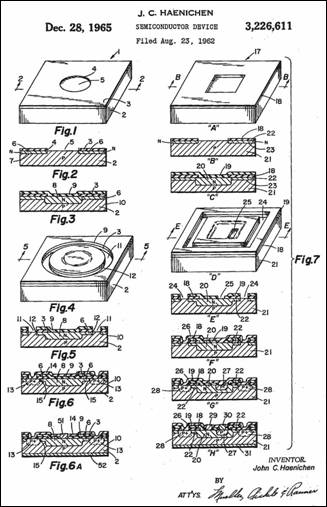
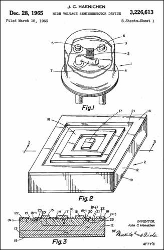
Above are sections of two of the key patents granted to Jack Haenichen that characterized the annular process. At left is one of Jack’s earliest patents, 3226611, which states in part: “This invention relates to stabilized or passivated silicon semiconductor devices and more particularly to a method of fabricating stabilized planar NP silicon diodes and PNP transistors suitable for high voltage operation”. At right is related patent 3226613 which states: “This invention relates to semiconductor devices and particularly to passivated transistors and other semiconductor devices having improved high voltage operating characteristics”. Both of these patents (and the other related Haenichen patents listed on page 16 of the Oral History) provide a wealth of information regarding the specifics of the annular process. This work was fundamental in establishing a more robust transistor structure, and has been the basis for silicon semiconductor manufacture ever since. It is interesting to note that Jack’s patents reference other patents that had been previously granted to a few of the early pioneers in semiconductor history, specifically Shockley, Teal, Fuller, Atalla, and Hoerni. Jack’s contributions can be seen as providing a fundamental improvement of the existing transistor processes of the time.
Go To Haenichen Oral History, Page 11
|
|
|
COPYRIGHT © 2007 by Jack Ward. All Rights Reserved. http://www.transistormuseum.com/ PAGE 10 |
|